

Scandium aluminum nitride (ScAlN) is a novel materials that would make these transistors higher as it may well improve provider focus.
“It displays massive polarisation, which will increase electron densities within the two-dimensional electron gasoline,” in line with the Tokyo College of Science. “Moreover, its ferroelectric nature makes it appropriate to be used as a ferroelectric gate materials in ferroelectric hemts. Such a gate permits dynamic management over the electron gasoline, providing potential to diversify the performance of GaN-based units.”
Nevertheless, it isn’t a simple materials to develop in a managed manner.
Sputtering could make it, however not at enough high quality, and molecular beam epitaxy also can succeed, however too slowly for manufacturing. That is in line with the Fraunhofer Institute for Utilized Strong State Physics (IAF) in Germany, which managed to make for the primary time utilizing production-friendly MOCVD again in 2019, attaining ~600cm2/V/s mobility and ~4 x 10¹³/cm2 provider density.
This MOCVD course of is now patented, and Fraunhofer IAF together with different establishments reported an electron gasoline provider density of 5 x 10¹³/cm2 on the Worldwide Convention on Nitride Semiconductors this 12 months.
Tokyo College of Science is speaking about ScAlN in the present day as a result of it has revisited sputtering, discovering that prime temperature is the important thing to enhance sputtered ScAlN skinny movie epitaxial on AlGaN-AlN-GaN heterostructures.
“In comparison with costly and sophisticated deposition methods, sputtering, broadly utilized in electronics manufacturing, can allow the mass manufacturing of ScAlN skinny movies at a lot decrease prices, making high-performance units extra accessible,” mentioned Tokyo researcher Atsushi Kobayashi.
They have been 10% scandium movies, studied utilizing atomic drive microscopy, electron diffraction and Corridor-effect measurements.
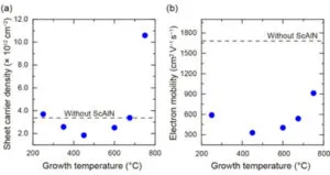
Floor flatness of the movies improved above 250°C and, at 750°C, step-and-terrace options appeared suggesting excessive structural high quality beneath.
Service density within the 2-d gasoline within the pattern grown at 750°C reached 1.1 x 10¹³/cm2,” roughly thrice that of AlGaN-AlN-GaN heterostructures with out ScAlN”, mentioned the college, whereas movies grown at decrease temperatures have been worse than with out ScAlN (see graph).
Electron mobility within the 750°C Tokyo ScAlN-inclusive samples was ~900cm2/V/s, nonetheless decrease than 1,677cm2/V/s scored by the group’s non-ScAlN reference – attributed by the researchers to roughness and structural imperfections launched by the ScAlN barrier.
“Our research demonstrates the viability of sputtering for rising high-quality ScAlN layers on GaN, providing a sensible path in the direction of the commercialisation of GaN hemts with ScAlN boundaries,” mentioned Kobayashi.
The work is printed as ‘Impact of progress temperature on the structural and electrical properties of sputter-epitaxial ScAlN on AlGaN/AlN/GaN heterostructures‘ in APL Supplies – may be learn in full with out fee.
Final 12 months, Tokyo Tech turned to scandium for ferroelectric reminiscence supplies