
Information storage in NAND flash reminiscence is a fancy course of that’s not solely obscure, but additionally difficult to clarify. People are good at abstraction, and we use this talent to boost expertise, even when we aren’t conscious of what’s precisely occurring on the degree of matter. Within the case of NAND flash, we perceive it on completely different ranges. We begin from probably the most fundamental unit of reminiscence, the reminiscence cell whether or not floating gate or cost entice, after which we dig deeper. We then get into the chemical construction and go all the way down to the atomic degree. It’s an attention-grabbing expertise. Scientists and Engineers have completed an unimaginable job of utilizing electrical cost to retailer knowledge inside these nanoscopic cells. Are we confused but? Don’t be… this may all fall into place.
Once we make use of NAND flash in sensible purposes, like SSDs for example, there’s a lot to look at. One of the vital frequent concepts is that of storage density. Storage density determines what number of bits of knowledge will be saved inside a single reminiscence cell. In our first article of ‘Studying to Run with Flash 2.0’ , we look at and attempt to present considerably of a fundamental understanding of NAND varieties, together with the give and take of every.
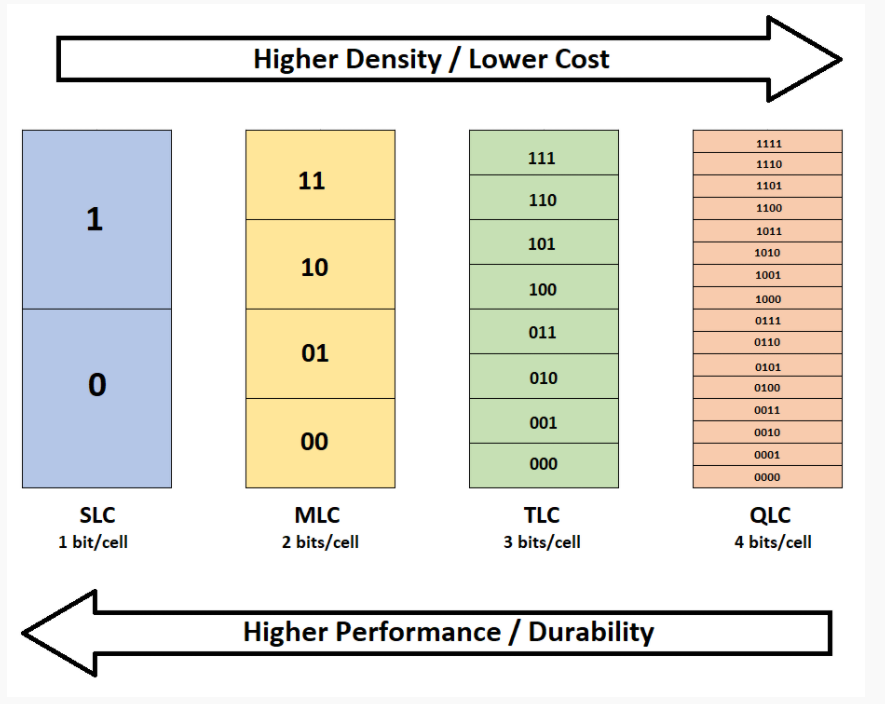
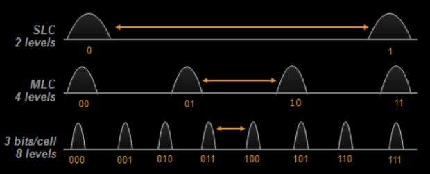
On the premise of storage density, NAND flash is on the market in 4 varieties. These are SLC (Single-Stage Cell), MLC (Multi-Stage Cell), TLC (Triple-Stage Cell), and QLC (Quad-Stage Cell). Penta-Stage Cell is already in improvement, however for now, now we have these 4 to speak about.
WHAT IS A MEMORY CELL IN NAND FLASH?
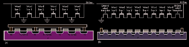
NAND flash is a non-volatile reminiscence, however the time period “reminiscence” is technically incorrect. On this reminiscence, the info continues to be current and intact, even when the enter energy is lower. Nevertheless, we historically name it a reminiscence cell, and there’s no hurt in that. How a reminiscence cell shops the info is a really attention-grabbing phenomenon of physics. The reminiscence cell is made up of a transistor. Historically, it was a floating-gate transistor however trendy SSDs make the most of charge-trap flash, which will be thought of a contemporary variant of the identical expertise. It simply has higher charge-holding and therefore knowledge retention capabilities.
So, now we have a reminiscence cell made up of a transistor, and it may maintain a really small quantity of cost inside two layers of insulator materials. In the event you perceive the traditional transistor , you’d know that it may work as a swap. Two terminals can permit or disallow the circulation of present relying on the standing (On/Off) of the third terminal, referred to as a gate. The voltage (threshold) at which the transistor opens or closes is fastened and might’t be modified. {n the case of a floating gate transistor, some extra layers are added, and it modifications the brink voltage. This variation occurs as a result of cost that’s saved between these insulating supplies (referred to as the floating gate in FGMOS). Totally different ranges of cost on the floating gate pose completely different variations within the threshold voltage.
The controller in your SSD has many roles, however one in every of its elementary roles is to detect this threshold voltage or a change in it. For instance, it might be programmed to detect “0” when the brink voltage is greater or “1” when the voltage is decrease.
Once we mix actually billions of those cells, we are able to create an enormous array of cells that may retailer a really massive variety of these 0s and 1s. These 0s and 1s are higher often called…knowledge. Let’s check out every cell kind, as we would determine them with SSDs, and look at the great…and never so good of every.
#1 – SLC (SINGLE LEVEL CELL)
SLC has probably the most fundamental kind of design amongst all NAND flash varieties. One cell can maintain both 0 or 1, and in outcome, is the quickest and most dependable of all kinds. Think about this as a swap, off or on. It is usually the most costly as a result of it doesn’t make the most of the total capabilities that every reminiscence cell has. It’s reserved solely for enterprise SSDs as a result of excessive price and steady operation capabilities. We do see SLC used as SLC cache in some shopper SSDs whereas, TLC or QLC have turn out to be main storage medium at the moment.
This picture is one in every of our first of SLC NAND and brought by Paul Alcorn for his report means again in 14 March 2012. It’s of the Toshiba MK4001GRZB 400GB SAS 6Gb/s Enterprise SLC SSD.
SLC NAND flash is reserved for knowledge facilities, servers, and different forms of enterprise storage, not due to the efficiency however due to the upper endurance as nicely. SLC NAND flash gives an distinctive endurance starting from 50,000 to 100,000 Program/Erase cycles.
If we have a look at the design, SLC has solely two discrete voltage ranges, i.e., excessive/low or 0/1. A single reminiscence cell can have one in every of these two states, and it both represents a bit worth of 0 or 1. To retailer and retrieve the info, very fundamental algorithms are required within the controller. Put on-leveling, rubbish assortment, and TRIM are a lot simpler to implement.
WHY DON’T WE SEE SLC NAND IN SSDS TODAY?
The primary REASON is the price. aS SLC nand is THE most costly per GB, it’s not cost-effective for large-scale client storage purposes. The second trade-off is the decrease capability on the identical chip dimension in comparison with different forms of NAND flash. slc nand is used extensively in enterprise, aerospace, industrial, and protection purposes. So, it’s hardly out there for different purposes.
#2 – MLC (MULTI-LEVEL CELL)
As we had defined above, SLC has the only design as a result of a single reminiscence cell is used to retailer one bit of knowledge. With MLC, the complexity will increase as now, a single cell is used to carry two bits of knowledge. The variety of discrete voltage ranges will increase. As a substitute of both excessive or low voltage, the cell can have two extra ranges in between. By way of bit values, it may have one of many 4 distinctive bit mixtures, i.e., 00, 01, 10, or 11. The storage density will increase by 100% however the bodily footprint stays the identical.
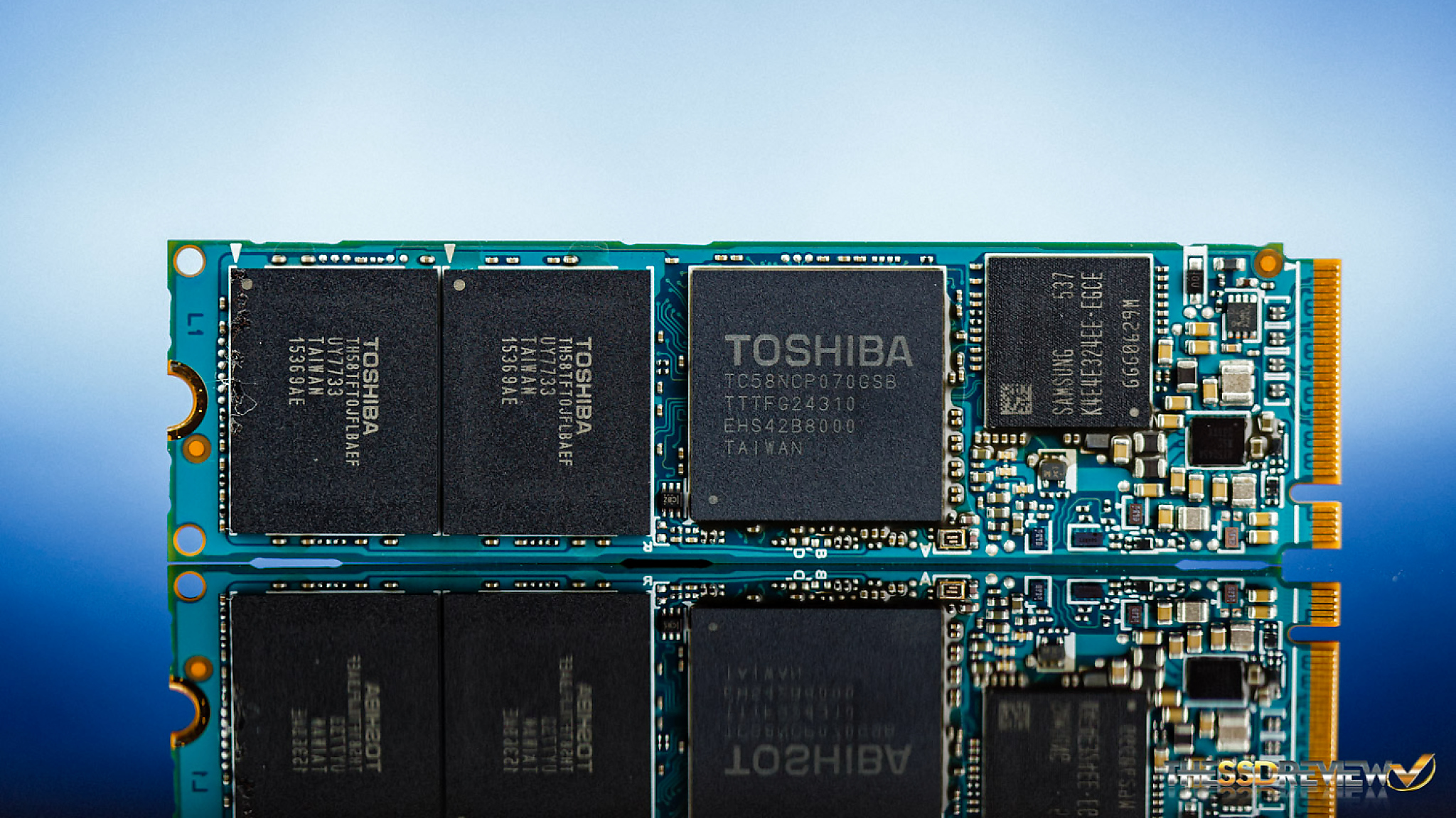
This picture depicts Toshiba MLC reminiscence within the OCZ RD400 from our report on 24 Might 2016.
MLC NAND flash is usually reserved for enterprise SSDs because the 3D stacking in TLC and QLC gives virtually comparable endurance and efficiency at a decrease price. This was out there in older client SSDs like Samsung 970 Professional, Toshiba OCZ RD400, and Samsung 860 Professional, however at the moment, it’s uncommon to see. If we discuss endurance, MLC can supply 3,000–10,000 Program/Erase cycles. The quantity decreased due to the elevated put on on the cell and the complexity of dealing with that knowledge.
SO WHY NO MLC NAND IN SSDS TODAY?
With elevated storage density, we commerce off the endurance considerably in comparison with SLC. MLC NAND flash is slower than SLC, error charges are greater, and its excessive price to fabricate limits client manufacturing.
#3 – TLC (TRIPLE LEVEL CELL)
Triple-Stage Cell can retailer 3 bits of knowledge per cell. This implies now we have 8 doable voltage ranges. From MLC, the storage density is elevated by 50% and 200% from SLC. This elevated cupboard space is usually thought of a great compromise between the SLC’s excessive endurance however excessive price and QLC’s low endurance and low price. Usually, TLC NAND flash has endurance between 1,000 – 3,000 Program/Erase cycles. To handle this low inherited endurance, producers depend on DRAM cache, TRIM, rubbish assortment, write cache, and varied different strategies.
TLC is especially utilized in client SSDs as MLC has turn out to be out of date within the shopper market. With the assistance of 3D stacking, it may be scaled considerably and nonetheless supply good reliability. To enhance its uncooked efficiency, particularly in write eventualities, producers typically make use of a pseudo-SLC cache the place the identical TLC cells are utilized in SLC mode.
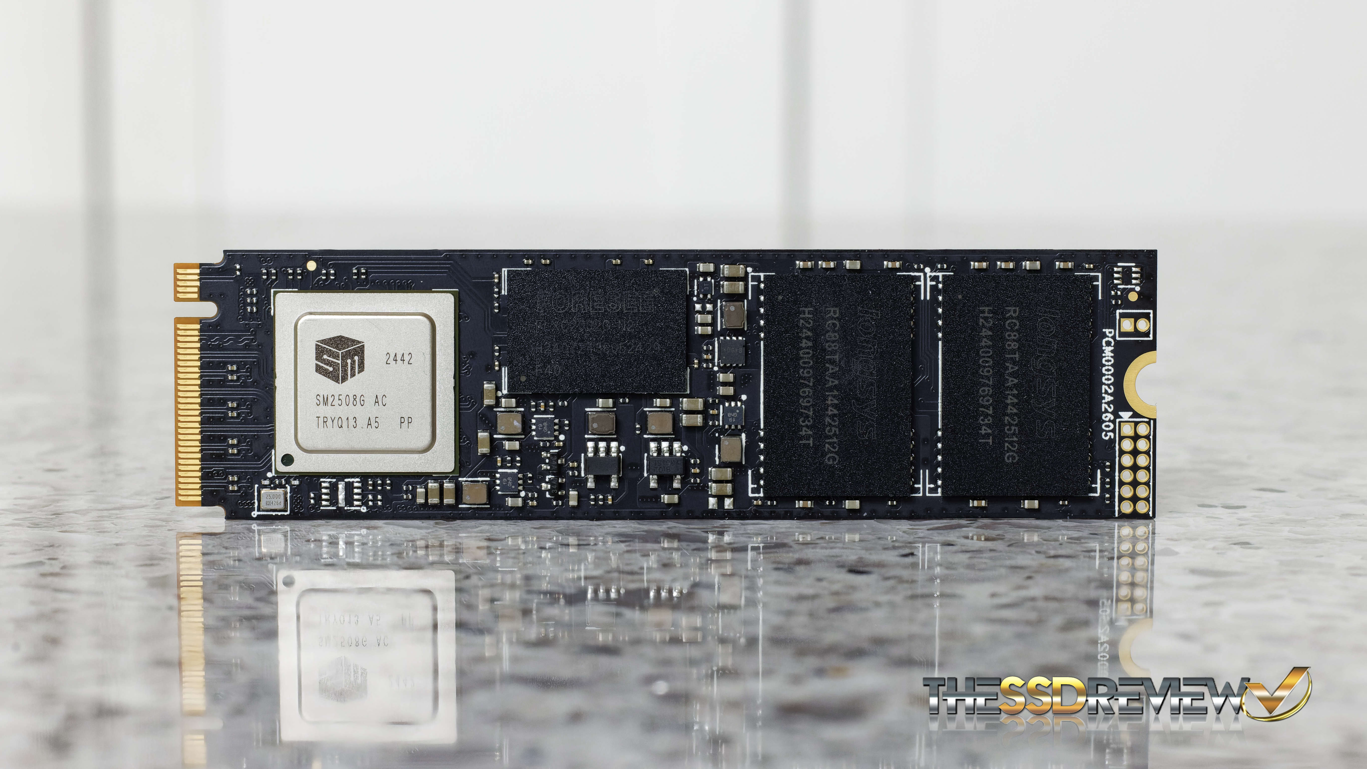
This picture is from one in every of our newest experiences on the Lexar 1090 professional Gen5 2TB SSD which makes use of Longsys branded Micron’s 232-layer 3D TLC B58r Fortis Flash NAND flash reminiscence.
TLC NAND FLASH TRADE-OFF
For the elevated storage density and decrease cost-per-GB, we commerce off the endurance. there are additionally extra errors and better write amplification. As a result of a single cell is being overused in comparison with SLC and MLC, TLC has a decrease lifespan as nicely. Slower write velocity is one more disadvantage due to the upper variety of exact voltage ranges inside a single reminiscence cell.
#4 – QLC (QUAD LEVEL CELL)
Till now, QLC has demonstrated the best degree of storage density amongst all forms of NAND flash. A single cell can maintain 4 bits of knowledge with the 14 completely different doable voltage ranges. You possibly can think about the extent of complexity and the software program refinements, like ECC, required to deal with errors. In QLC, the storage density will increase by 33x from MLC and 4x that of SLC. To take care of knowledge integrity, LDPC (Low-Density Parity-Examine) is a should. An excellent heavier and bigger SLC write cache is employed to compensate for the extraordinarily low uncooked write velocity. QLC typically has endurance of 100-1000 Program/Erase cycles.
QLC is used closely in client environments the place storage density at decrease costs is the precedence. One other main use that has emerged is with AI coaching, the place knowledge integrity isn’t as necessary as the scale of the datasets. QLC SSDs assist lots in saving budgets for AI knowledge and coaching corporations.
WHY ISN’T QLC MORE COMMON IN SSDS?
In trade for the best storage density and lowest price per GB, we get a significant drawback of decreased endurance and lifespan. As a result of a single reminiscence cell is used to carry 4 bits of knowledge, the write efficiency may be very low, primarily as a result of precision required to keep up that brief voltage window. All in all, QLC NAND flash is most well-liked the place cupboard space is prioritized over reliability.
FINAL THOUGHTS… AND A BIT OF A REQUEST
That is our first article in our new collection “Studying to Run with Flash 2.0”. It could be very useful if readers shared their suggestions or solutions within the feedback, as this may help in our route for future posts. Constructive criticism is all the time welcome. Our plan is to cowl a big selection of SSD subjects. If you need us to cowl something particularly, we’re ready to your phrases.
Thanks for studying!
That is the primary article of we hope to be many from our latest addition at The SSD Assessment, Anshul Rana. Anshul has a B.E in Electronics and Communication Engineering and in addition has his personal web site at www.storedbits.com. Superb Work Anshul and Welcome to TSSDR!