
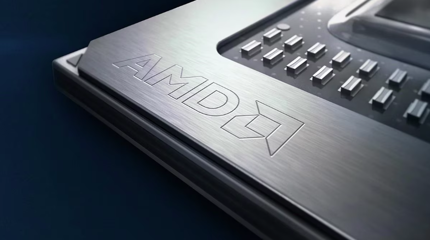
AMD introduced that its next-generation EPYC processor, codenamed “Venice,” has entered manufacturing on TSMC’s 2nm course of in Taiwan. The corporate additionally plans to broaden manufacturing at TSMC’s Arizona facility, signaling a broader technique to diversify its advanced-node capability and scale provide for cloud and AI deployments.
“Venice” is positioned as the primary HPC-class processor to ramp on TSMC’s 2nm node. The transition to 2nm is predicted to enhance efficiency per watt and transistor density, each of that are essential for information heart operators dealing with energy and cooling constraints. AMD framed this milestone as a part of its ongoing EPYC roadmap execution, with a deal with enabling larger core density, improved effectivity, and tighter integration throughout compute subsystems.
Venice can also be anticipated to introduce the brand new SP7 socket, a bodily bigger platform than the outgoing SP5 that’s designed to accommodate larger energy supply, extra reminiscence channels, and expanded I/O bandwidth to assist considerably larger core counts per socket.
CPU Function Expands with AI and Knowledge Heart Orchestration
AMD emphasised that CPUs stay central to fashionable AI infrastructure, whilst accelerators deal with mannequin coaching and inference. In manufacturing environments, CPUs orchestrate information pipelines, handle storage and networking stacks, implement safety, and coordinate distributed workloads. As AI evolves towards extra complicated agentic workflows, these duties broaden, inserting extra calls for on CPU efficiency, reminiscence bandwidth, and I/O.
The “Venice” ramp aligns with this shift. By leveraging the 2nm course of, AMD is concentrating on effectivity and throughput good points that assist large-scale AI clusters and conventional enterprise and HPC workloads. The corporate continues to see momentum in EPYC adoption throughout hyperscale and enterprise environments, the place consolidation and vitality effectivity stay key shopping for standards.
Manufacturing Technique and TSMC Partnership
Preliminary manufacturing in Taiwan will likely be adopted by a deliberate ramp-up at TSMC’s Arizona fab, reflecting AMD’s effort to steadiness modern manufacturing with geographic resilience. This method is more and more related to enterprise patrons, given provide chain and regulatory issues in information heart infrastructure sourcing.
AMD and TSMC proceed to collaborate on course of and packaging applied sciences. Along with the 2nm node, AMD is leveraging superior packaging applied sciences, together with SoIC-X and CoWoS-L, throughout its broader information heart and AI portfolio. These applied sciences allow higher-bandwidth interconnects and tighter integration amongst compute dies, reminiscence, and accelerators, which at the moment are customary necessities for AI-optimized platforms.
Roadmap Outlook with “Verano”
Trying forward, AMD plans to increase its use of TSMC’s 2nm know-how with “Verano,” recognized as a sixth Gen EPYC processor. Verano is predicted to ship enhancements in efficiency per greenback and per watt, with design optimizations for cloud and AI workloads. AMD additionally indicated assist for superior reminiscence applied sciences, together with LPDDR, which may enhance energy effectivity and reminiscence bandwidth in scale-out deployments.
Verano is predicted to undertake the brand new SP8 socket, which succeeds at this time’s SP6 and targets a extra typical energy envelope. SP8 is positioned for mainstream and entry-level server deployments, retaining a extra acquainted thermal profile whereas nonetheless benefiting from the transfer to 2nm, next-generation I/O, and up to date reminiscence assist. The 2-socket technique provides AMD broader protection throughout the information heart stack, with SP7 addressing most efficiency necessities and SP8 supporting power-conscious and cost-sensitive footprints throughout general-purpose enterprise and edge infrastructure.
The Venice ramp and the Verano roadmap underscore AMD’s continued funding in CPU innovation as a foundational layer of AI infrastructure. Whereas GPUs and accelerators dominate headlines, the CPU stays a essential management aircraft for information motion and system orchestration. Developments in course of and packaging will immediately form how effectively next-generation information facilities scale compute, storage, and networking assets.
With Venice getting into manufacturing, Verano on the horizon, and two new sockets reshaping the platform panorama, the processor section is ready for a very lively stretch. We’re wanting ahead to what AMD has in retailer at AMD Advancing AI 2026, the place the subsequent part of this roadmap is predicted to return into sharper focus.