
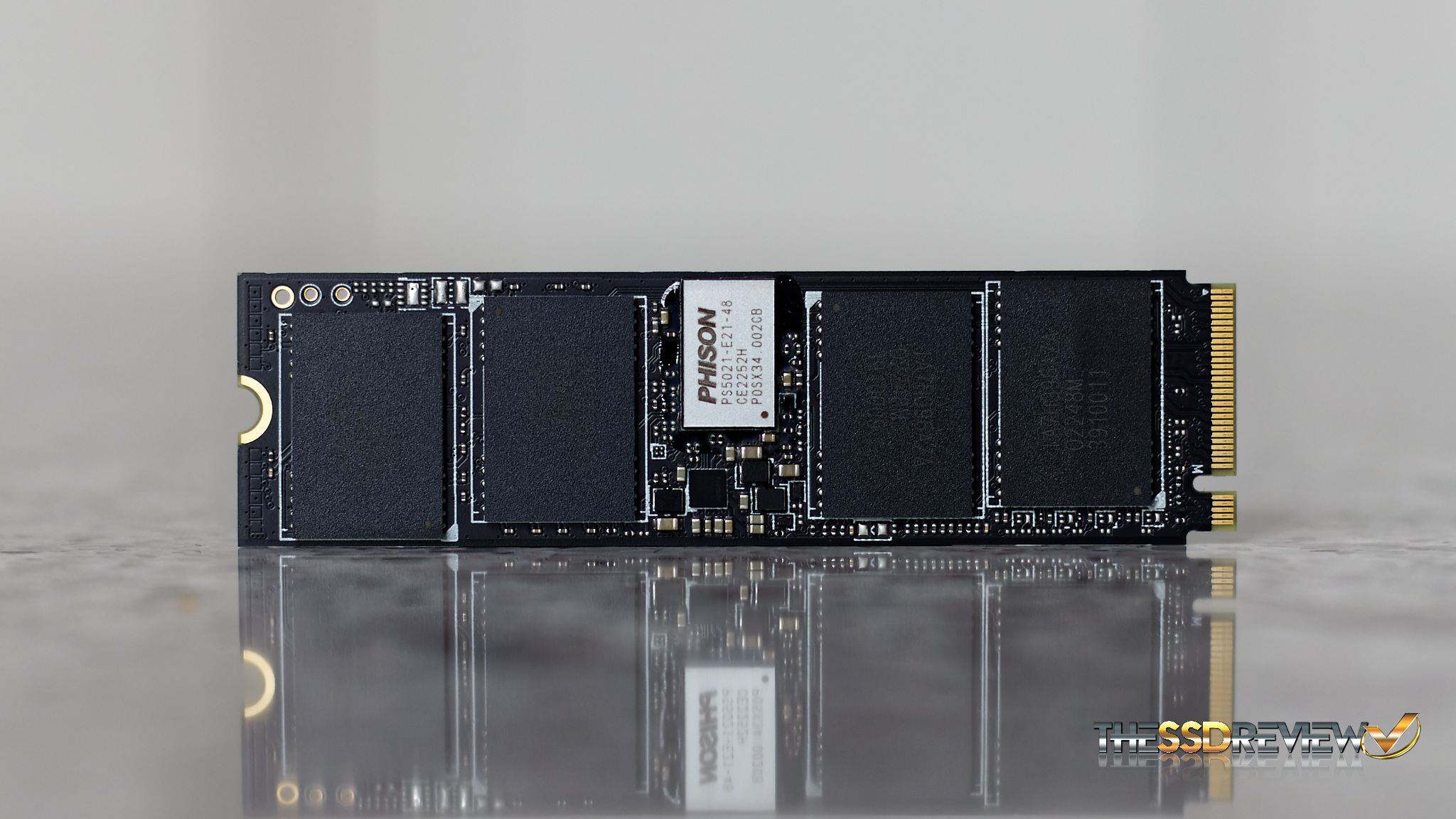
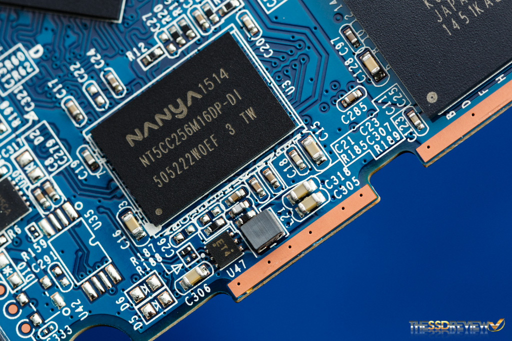
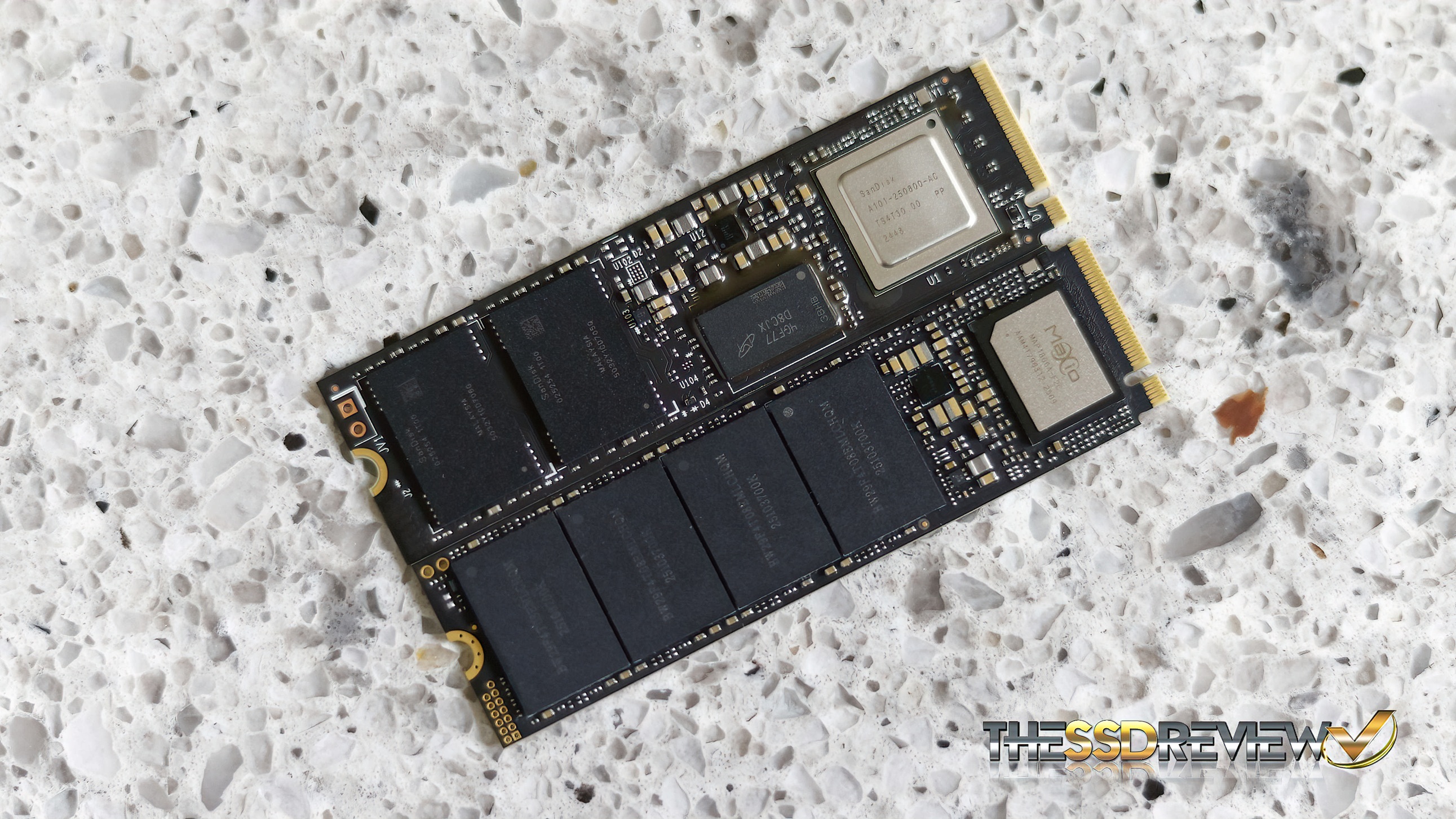
After NAND Flash and controller, DRAM is maybe a very powerful element on an SSD. In our premier article of our latest ‘ Studying to Run with Flash 2.0’ entitled, ‘Understanding SLC, MLC, TLC and QLC NAND Flash‘ we supplied an understanding of the various kinds of NAND and worth of every within the SSD spectrum. Right this moment, we’ll be taking a step additional and discussing DRAM vs DRAM-less SSD designs. DRAM in SSDs serves many roles, a very powerful being the storing and managing of information constructions, such because the Flash Translation Layer (FTL). Sounds complicated proper? Observe alongside and we’ll make issues easy.
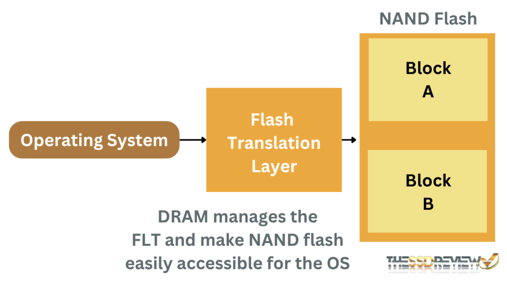
Contemplate the FTL just like an Index in a ebook that allows you to get to a chapter in a short time. FTL maps the logical block tackle (utilized by working techniques) to bodily areas on the NAND flash. In easy phrases, it’s a mapping desk that retains monitor of the place particular knowledge is positioned on that NAND. DRAM ensures the controller has quick entry to this desk, permitting it to find the information rapidly at any time when required. Moreover, DRAM on an SSD serves as a high-speed knowledge buffer, serving to to cut back latency and improve total NAND flash efficiency.
DRAM is a helpful element of SSDs, however is not needed since Home windows 10, actually, when HMB got here into play. Right this moment, SSDs can make the most of the system’s RAM as a Host Reminiscence Buffer, or HMB. SSDs that use HMB relatively than a bodily DRAM chip are often known as DRAMless SSDs. These designs are sometimes applied on price range drives.
As an alternative of the on-chip DRAM, the controller and working techniques divide some area from the system’s major reminiscence and assign it as an HMB. There are some drawbacks of DRAM-less SSDs, akin to increased latency and slower learn pace. On this article, we’ll converse to points regarding DRAM-less SSDs and why they’ll typically be an excellent choice. Let’s begin by understanding the aim of DRAM (Dynamic Random Entry Reminiscence).
WHAT IS THE PURPOSE OF DRAM IN AN SSD?
DRAM is a high-speed cache or buffer between the host system and the NAND flash. As DRAM has very low latency and really excessive uncooked learn/write pace in comparison with NAND flash, it’s excellent for dealing with the incoming heavy streams of information. This gathered knowledge can then be saved within the everlasting NAND within the background. To be able to work along with the host, the mapping tables should be rapidly accessed and re-updated. DRAM, with its excessive uncooked learn/write pace, helps the controller have entry to the FTL.
UNDERSTANDING THE FILE TRANSLATION LAYER (FTL)
NAND cannot be written to an SSD instantly. It should be erased on the block degree after which written on the web page degree. The NAND programming mannequin mandates {that a} web page can solely be written as soon as it has been erased. If a web page is partially stuffed and we have to replace it, the brand new knowledge can’t be written to the identical web page; as a substitute, the up to date knowledge should be written to a brand new, clear web page, and the previous web page is marked as invalid. This course of is managed by the Flash Translation Layer (FTL).
Then again, the working system expects a linear array of Logical Block Addresses. It additionally expects a easy knowledge construction like a listing of blocks 0, 1, 2, and so forth. NAND Flash is essentially incompatible with this manner of information studying and writing. The flash translation layer (or index) assists the OS in using NAND flash with its personal methodology of information group.
FTL acts as a real-time translator. It makes the NAND flash seem as a traditional overwrite-capable and random-address block gadget. A major quantity of code runs within the background with processes like mapping tables being created and up to date, rubbish assortment, write redirection, and put on leveling. A 1TB SSD would usually require 1 million 4KB logical blocks with lots of of megabytes of metadata. To entry, create, replace, and delete this metadata, DRAM serves an necessary function and therefore makes our SSDs sooner.
HOW ELSE DO DRAM BENEFIT SSDS?
SSD DRAM performs a significant function in write buffering. Write buffering is the method the place newly launched knowledge is quickly held in a buffer earlier than its closing bodily write to its storage location. Because of SSD ‘erase-before-write’ restrictions, DRAM acts as a write cache and handles the incoming bursts of information quickly with its excessive learn/write pace.
DRAM and RAM are unstable, which means that the data is misplaced as soon as the ability is eliminated. SSDs are sensible with their ‘journal commits’ and capacitors that forestall knowledge loss if an influence failure happens. In these situations, if the system loses energy, the information nonetheless within the DRAM is moved to the NAND flash for everlasting storage. The following time the system is booted, that info is loaded again into the DRAM.
DRAM additionally helps with knowledge prefetching, which improves the learn pace, in addition to rubbish assortment and heap-leveling by permitting sooner map entry. All of the algorithms typically run within the background when the SSD is idle, which suggests, with DRAM entry, these background processes have little to no influence on SSD efficiency.
HOW DO DRAMLESS SSDS WORK?
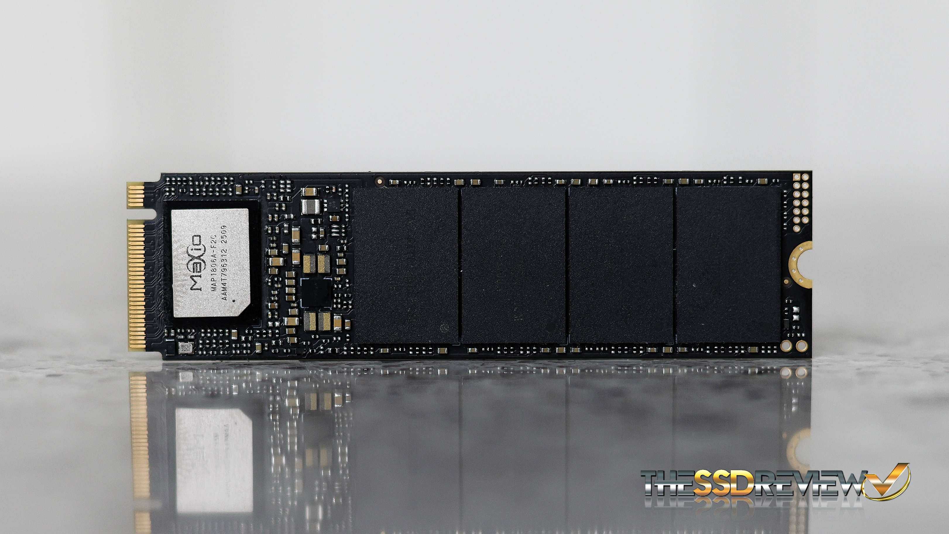
SSDs can perform completely with none onboard DRAM or HMB by storing their mapping tables instantly in NAND Flash. This was frequent in most SSDs earlier than 2014, particularly in lower-cost fashions, nevertheless, accessing these tables from NAND is slower and fewer environment friendly than utilizing DRAM. Host Reminiscence Buffer was launched in 2014 with the discharge of NVMe 1.2. It started to get adopted in shopper SSDs between 2015 to 2017. Right this moment, almost all DRAM-less SSDs depend on HMB, so our dialogue will concentrate on DRAM-less SSDs that use the HMB mechanism.
BORROWING A CHUNK OF DRAM FROM THE HOST SYSTEM
In DRAM-Much less SSDs, SSDs quickly use a small a part of the pc’s major reminiscence (RAM) and use it as a substitute for DRAM. This request is distributed by the NVMe protocol simply when the system boots. This portion is at all times shared throughout a recent boot and when the system shuts down, the information on the DRAM is saved within the NAND flash for everlasting storage. This course of occurs once more within the subsequent boot.
The SSD’s built-in software program (referred to as firmware) works with the working system to set all the things up by the NVMe driver. The scale of acquired RAM is mostly dynamic and varies primarily based on the capability of the drive and the duty at hand.
As soon as the system grants entry to this reminiscence, it’s not obtainable for the system. This entry is given by way of the PCIe bus utilizing Direct Reminiscence Entry or DMA. DMA permits the SSD to learn and write knowledge to and from the host reminiscence with out a lot interference from the CPU. Think about it as a bypass to the DRAM. The identical sort of information, like FTL mapping tables, write buffer, learn cache, and different metadata, is saved within the HMB, however its location modifications.
MAJOR DRAWBACKS OF DRAM-LESS/HMB DESIGN
As in comparison with the Onboard RAM, HMB is slower. This makes the DRAM-less SSDs slower by design in sure duties. The important thing drawbacks are increased latency, slower efficiency in random learn/write duties, and elevated write amplification. DRAM-Much less SSDs even have much less constant efficiency throughout sustained use.
Although PCIe lanes are quick and the most recent developments in HMB are superb, the extra steps and the elevated distance between the system RAM and NAND cut back the entry pace and improve the latency. The impacts might be seen primarily in excessive IOPS duties. HMB permits a restricted reminiscence dimension in comparison with what the producers give on the onboard DRAM chips.
You would possibly suppose, why don’t we tweak the firmware and use extra of the system reminiscence as HMB? That isn’t attainable with out the willingness of the host system and NVMe specs. Additionally, the dimensions of HMB doesn’t at all times assist, particularly when low latency and excessive DRAM efficiency are required to get issues finished. The small dimension of HMB usually leads to lesser efficiency after we work with massive quantities of information.
I’ve the Kingston A400 in my previous laptop computer, and it really works simply positive when I’m doing something informal. In combined or heavy workloads like when I’m working a digital machine or compiling massive codebases, I can clearly observe the distinction when in comparison with my major system with a DRAM primarily based SSD. The same old efficiency impacts are dropped IOPS and elevated latency.